PC110 TFT���p���p��@���C�@�@�@�mto English Note�n

�{�{�{�@�F�ѕ\���̉��P�@�{�{�{
Moonlight����̒Nj��͂̂��A�ŁA�uPC110�v�̐F�M���[�q�̐���������U�肪���������B�i���C�����ڑ��}�j
����ɏ]���āA��z����1�������u���p��v���������A�����Y���"3x256�F��"������ꂽ�B
���L�̎c��̃}�V�����A�����ڑ��̂܂܂ɂ��Ă����̂��A�C�����������̂ŁA�v�����āu���p����v����蒼�����Ƃɂ����B
�ŏ��A���q�������̂́A"�r�A�ƃr�A�E�z�[���i�r���E�z�[���ł͂Ȃ��I�j�̑傫���h���A�v���ʂ�ɏk�߂��Ȃ��������ƂŁA�C���C�����Ă����B
�����A���S�ɖ߂��āA�匳��"��Z�b�g�A�b�v"�̏��ŁA�������͂��̑傫���܂ŏk�߂Ă����A���"�l�b�g�N���X�̃T�C�Y"���w�肷��A����I�ȑ傫���^�������ő������邱�Ƃ����������B�i���������I�j
�������A�F�X���s�̘A���B
��Ɂu��H�}�v�i�}�Q<�N���b�N>�j��`���Ă���A��ŁA�u���C�A�E�g�}�v�����n�߂���A����Ɏ肪�����āA�u��H�}�v�Ƃ͂��Ȃ�Ⴄ�ڑ��ɂ��Ă��܂��Ă����B
�Ƃ��낪�A�u��H�}�������X�V�v�Ƃ����R�}���h����������A�h�h�b�Ɓu���C�A�E�g�}�v�������_�������Ă��܂����I�H
�D�D�D��u�A���R�E�ځ[����E���R�B�i����ȃJ�z�i�I�j
�܂��A���������ɂ���A�����͎̂����g�I
�D�D�D��������A�G�b�`���I�b�`���A�Č���ƁB
�D�D�D�ŁA�ꉞ�͏o�����̂����A����͊�̑傫�������Ă��āA�i����Ȃɑ�R�͕K�v�������̂�����ǁA�j�������悹�悤�Ǝv���Ă���B�i�}�P�j
�i���A��ɁA����A�����z������点�Ă݂��̂����A�₽��N�l�N�l�ƋȂ������z�������o���Ȃ��炵���̂ŁA�����z���͎~�߂��B45�x�X�ΐ��𑽗p���Ă���̂ŃR���p�N�g���̖ʂł́A�D��Ă���悤�����A�菑���̒P��������"�������肳"�ɂ͏��Ă܂��I�j
FMI�iFor my Information ?�j�F���܂ŖY��Ă����̂����A�uAT050TN22 V.1�v�̑O�g�́uAT050TN22 �iV.0)�v�́A�g���Ղ��i40�s���[�q�́j�uVGA�|TFT���W���[���v�������͂��Ȃ̂ŁA��������̍ɂ�����ATFT���������y�Ȃ��Ȃ��B
���邢�́A������������̃}�V���ɓ��ڂ���Ă����͂��Ȃ̂ŁA���̏��i���W�����N�i�Ƃ��Ďc���Ă���A���p�o���邩������Ȃ��B
�ʂ����āA������T�����Ă��邾�낤���H
�|�|�|�|�|�|�|�|�|�|�|�|�|�|�|�|�|�|�|�|

�{�{�{�@�lj���H�@�{�{�{
����A�P�x�����̉�H�������������A���i����ɓ�������ڂ��Ă݂悤�ƁA�p�^�[���ɒlj������B
�V�~�����[�g�����̂́A5�^VGA������A6�^WVGA�Ȃǂł́u�萔�v���قȂ邩������Ȃ��̂ŁA�ŏI�I�ɂ́A�ׂ��ȍ��킹���݂��K�v���낤�B
�g��Ȃ����ɂ́A�W�����p�[�̕����q���ł����ςށB
�i�D�D�D�Ƃ����܂ŏ����āA�͂āH"�ی��R"�͕K�v�Ȃ������̂��ȁH�Ǝv���t���Ă��܂����B���́A���܂�"�ی��R"�͈�ؓ���Ă��Ȃ������̂����A�܂����̂͋N���Ă��Ȃ��B�����A�d���ׂł��邱�Ƃ͊ԈႢ�Ȃ����낤�j
�W�����p�[�̑���ɁA"�ی��R"�ɐ�ւ�������̕����A������������Ȃ��B
�܂��A���x���̌���lj����K�v���낤����A�u�����v�͂���������ɂ��悤�Ǝv���B
PC110 TFT���p���p��@���P�@�@�@�mto English Note�n

�{�{�{�@+22V�d���̓d�������̖��@�{�{�{
�ŋ߂́A���̞B����TFT���̏�Ԃ��AMoonlight����Ɍ���߂��邱�Ƃ����X����B
�����"��ʓI"�ȍl�@�ƌ���������A���͊��}���Ă���B
�uPC110�v�́u�F�o�͐M���v�̉��P�̌������������A����́A�uLED�o�b�N���C�g�v�̓_���Ɏg�p����ƁA�u+22V�d���v���ߕ��ׂɂȂ�߂����댯�ł͂Ȃ����Ƃ��������B
�i���̓d���́A���ۂɂ́uFn+Ins�v�L�[�ōő�܂ŏグ��ƁA��+27V�߂��܂ŏオ�邱�Ƃ��������Ă���j
����ŁA�i�d���͑����Ă��Ȃ��������j�u�o�b�N���C�g�v��_��������ƁA���̒[�q�d������7V�`9V�ɂ܂Œቺ����B
����́A�d���e�ʂ����Ȃ��d���́A������R�������̂ŁA�d���𑽂����o���ƁA�}���ɓd�����ቺ����̂��B
�i�́A�ǂ��g���Ă����u�g�����X�^AC�A�_�v�^�v���A���̃^�C�v�ŁA�����ׂ��Ɠd�����w��ȏ�ɍ����āA����̓d���𗬂��ƁA�\��̓d���ɂȂ���̂������j
�ł��A���̕��@�́A�d�����̔��M�������Ȃ�̂ŁA���܂��ǂ��Ȃ��g�����ł͂���B
������AMoonlight����̔��Ă������̂����A"�o�b�N���C�g�P�x���ςɂ�����"�Ƃ������ƂŁA�������ȈՌ^�u�d��-�d���ϊ���H�v���쐬���Ă݂��̂����A���ꂪ�A�i�^�ǂ��H�I�j�u+22V�d���v�̉ߕ��ׂ��y���o����@�\�����悤�ɂȂ��Ă����B�i�}�T�A�}�U<�N���b�N>�j
�d�����̔��M���́A�O�t���́u�_�[�����g���E�g�����W�X�^Q1�v�Ɓu�d�����o��RR3�v�̕��ɕ��U�����킯���B
�Ȃ̂ŁA�K���A���̉�H���ڂ��悤�Ǝv�����B
�i�ܘ_�A�����Ɠd���e�ʂ̑����͂��́A"�C���o�[�^�p�d��+10V"���~�����ė��p������@�����邪�A���ƂȂ��A����ł����v�ł͂Ȃ����Ƃ�������������̂ŁA���̂܂ܐi�s�I�j
����́u���p��v��"���C"�́A"���P"���܂߂�̂ŁA�g�����W�X�^���R�́A���ۂɍw�����āA���ۂɓ��ڏo��������ɁAPCB�̃p�^�[����ύX�����B
�i�v�悵�Ă���5-inch VGA-TFT�p�́A�܂��ʓr�l���邱�Ƃɂ��āA����ɂ͋��ڂ��Ȃ��ł����j
�|�|�|�|�|�|�|�|�|�|�|�|�|�|�|�|�|�|�|�|

�{�{�{�@���C�A�E�g�@�{�{�{
�u�_�[�����g���E�g�����W�X�^�v�́A�^�ǂ������Ȃ��̂�����o���������B
�u�\�ʎ����p��R�v�́A�������ɂ��ꂽ"�����i"��I�B
�i���[�����ŁA��������킳��ẮA�^�}�����I����Ȃ��j
�i�����ɂ��ẮA�ʂ̋@��ɋL���ɂ���̂ŏȗ��j
�����̃T�C�Y�ɍ��킹�āA�uPCB�v���́u�t�b�g�v�����g�v�������������B�i�}�V�j
�����A����ɐ旧���āu��H�}�v���̃v���p�e�B�ŁA�u�t�b�g�v�����g�v�ɏC�������Ă��Ȃ������̂ŁA�܂��܂������ڂɑ������B
�i�Ƃ����Ă��債�����Ƃł͂Ȃ��āAPCB�̏�ŁA"��H�}���̃t�b�g�v�����g"���A����������t����ꂻ���ɂȂ邾���Ȃ��A���̗��R���������ċ���A���ł��Ȃ����Ɓj
���́uKiCAD�v�̑���ŁA�V���ɔ����i���������́j�������B
�}�E�X�́u�z�C�[���v�́A"�g��E�k��"�̓��������m�炸�ɁA��ϋ�J���Ă����̂����A�uShift�L�[�i��E���j�v�A�uCtrl�L�[�i���E�E�j�v���������邱�ƂŁA"�㉺���E��"���o���邱�Ƃ�m�����B
�܂��A����ł��s�ւ����A����Ă���A�傢�ɏ����邾�낤�B
���A�����"DRC�i�f�U�C�����[���`�F�b�N�j"�����s������A�G���[���炯�B�i�}�W<�N���b�N>�j
���l���Ă��A�G���[�ł͖����낤�Ǝv���̂����A��t�o�ė���̂ŁA����������I
�i�����A����Ő����o�����̂ŁA����������ʂ����I��j
PC110 TFT���p���p��@�����@�@�@�mto English Note�n

�{�{�{�@���蔭���@�{�{�{
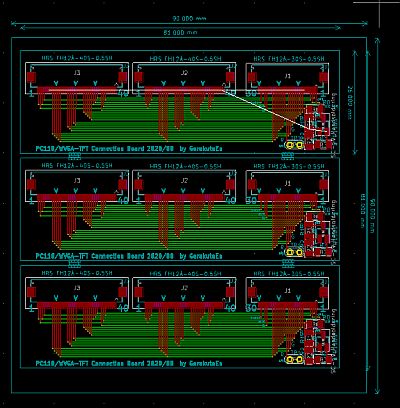
PCB�̏����b�g���Y�̕W���I�ȑ傫�����A100x100mm2�炵���̂ŁA����ɔ[�܂�悤�ɁA3���g�ɂ����B�i�}�X�j
�r�A�a�́A����4mm�����������A�א��Ƃ̊Ԋu�������ӏ����������̂ŁA�����3�o���ɂ��Ă݂��B�r�A�E�a��0.25mm�B�i�}�P�O<�N���b�N>�j
�o����A�r�A�a�ƃR�X�g���ׂ�����r���āA�R�X�g�p�t�H�[�}���X���グ���������̂����A������A�C���I�ȗ]�T�������āA�ȗ��B
��������Gerber�f�[�^�iSeeed�����Ɋg���q��ύX�j�F�b�� PC110_TFT_201.zip
����́A"PCBWay"�𗘗p���Ă݂悤�ƍl���Ă������A"WEB���ς���"������ƁA�W���ŁA���悻"$50"�قǂ��Ƃ����B
����ȂɊ|����̂��H�ƍ����S���������̂ŁA�����ɁA�O������"Seed/Fusion"�ł����ς���������Ă݂��B
��͂�A�������|����炵���B���������āA$62.64�i\6,960 JPY�j�������ȁB
�ǂ����A�r�A�E�a��0.3mm�����ɂȂ�ƁA���i��10�{�ɒ��ˏオ��炵���B
�����A10��$5�`$10��"������̔�"�̎����́A�߂����悤���B
�T�d�ɁA�������Ȃ��ƁA�₪�Ď���"PCB�j�Y"����I�����B�iT.T;?
****************************************************************
PC110 Relay board for TFT conversion

+++++ Improved color band display +++++
Thanks to the pursuit of Mr.Moonlight, the correct allocation of the color signal terminals of "PC110" was found. (Repaired connection diagram)
According to that, when I made only one "relay board" by hand wiring, a really beautiful "3x256 color band" was seen.
It is uncomfortable to leave the remaining existing machines with the old connection, so I decided to remake "relay board".
At first, I was frustrated that "vias and via holes(not bear hole !)size�h could not be shortened as desired. It was
However, if I go back to the beginning and reduce the size to the size that should be allowed in the original "board setup", then specify "net class size" to make it uniform size/small size. I found that they can be arranged in. (yare yare !)
However, a series of failures.
When I draw "Circuit diagram" (Fig_2 <click>) first and then later start to make "Layout diagram", my hands will move and I made a connection much different from the one shown in the figure.
However, when I pressed the command "Update board from schematic", lines and dots disappeared from "Layout"! ?
..... For a moment, I'm stunned, bozen, frightened. (Kahona ! / God and/or Buddah gone away !)
Well, no matter what I say, the bad thing is myself !
... From there, "Ecchila Occhila !", reconstruction work.
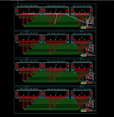
... Well, I was able to do it, but this time, considering the size of the board, I think that I will put multiple boards (though it is not necessary so much for myself). (Fig_1)
(In addition, I tried to do automatic wiring a few times earlier, but since it seems that only bent wiring can be made, automatic wiring is stopped. 45 degree inclined lines are often used. It seems that it is excellent in terms of compactness, but I can't beat the simple and clean handwriting!)
FMI (For my Information ?): I had forgotten it until now, but "AT050TN22 V.1"'s predecessor "AT050TN22" was supposed to be an easy-to-use (40-pin terminal) "VGA-TFT module".
If it's same size VGA, it's a lot easier to makeup TFTized "PC110".
Alternatively, it may have been installed on some machine, so if it remains as a junk item, it may be usable.
Can we find them ?
�|�|�|�|�|�|�|�|�|�|�|�|�|�|�|�|�|�|��

++++ Additional circuit +++
The other day, I examined a circuit for brightness adjustment, but I added it to the pattern so that I could put it on if I got it.
Since the simulation was a 5 type VGA, the "constant" may differ for 6 type WVGA etc., so in the end it will be necessary to make fine adjustments.
When not in use, just connect the jumper.
(... and so on, I end up thinking that I didn't need "protection resistance". Actually, I didn't include "protection resistance" at all, but the accident still occurred. It hasn't happened, but there is no doubt that it is a heavy load.
It may be better to switch to a "protection resistor" instead of a jumper.
It still needs some verifications and additions, so I'd like to place an "order" a little further.
PC110 Relay board for TFT improving

+++++ Current limitation problem of +22V power supply +++++
Recently, there are many cases where my ambiguous condition for TFTized "PC110" is exposed to Mr. Moonlight.
I'm welcoming because it is "quantitative" consideration and view.
As is the case with the improvement of "color output signal" of "PC110", this time, when used to light the "LED backlight", "+22V The power supply�h is overloaded and danger .
(This voltage is known to actually rise to about +27V when raised to maximum with the Fn+Ins key.)
By using this power line, (actually, I did not measured the current) the terminal voltage of the "backlight" has dropped to about 7V~9V.
This is because a power supply with a small current capacity has a high internal resistance, so if a large amount of current is taken out, the voltage will drop sharply.
(The "transformer type AC adapter" that was often used in the past was of this type, the voltage was higher than specified when there was no load, and when the specified current was applied, it reached the expected voltage.)
However, this method is less than bad usage because the power source generates a lot of heat.
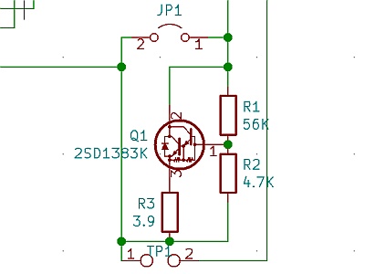
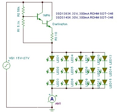
This time too, it was the idea of Mr. Moonlight, "He want to make the backlight brightness variable", so I tried to make a simple "voltage-current conversion circuit" , but it had a function to reduce the overload of (+22V power supply) (luckily ?!). (Fig_5 and Fig_6 <click>)
The heat generated inside the power supply may be distributed to the external "Darlington transistor Q1" and "current detection resistor R3".
So I definitely wanted to put this circuit.
(Of course, there is also a method of stepping down and using "Inverter power supply +10V", which should have more current capacity, but somehow I feel like it is okay at present, so proceed as it is.)
�|�|�|�|�|�|�|�|�|�|�|�|�|�|�|�|�|�|

+++++ layout +++++
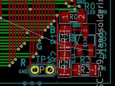
The "Darlington Transistor" is fortunately available at a low price.
For "Surface mount resistors", I have selected "special price products" that have been subdivided.
(Thousands of wound reels are not adequate for me !)
(I will omit these because I will write about them on another occasion.)
The "footprint" on the "PCB" side was rewritten to match those sizes. (Fig_7)
But before that, I didn't modify the "Footprint" in the properties on the "Schematic" side, so I had a terrible experience again.
(It's not a big deal, it's just that I'm almost forced to press the "schematic footprint" on the PCB, but if I know the reason, it's nothing. )
With this "KiCAD" operation, I made a new discovery (only for me).
The "wheel" of the mouse was very struggling, knowing only the function of "enlarging/reducing", but pressing the "Shift key (up/down)" and "Ctrl key (left/right)" at the same time.
Then, I learned that I can move up and down, left and right.
This is still inconvenient, but once I get used to it, it will be a great help.
If I execute "DRC (Design Rule Check)" again this time, there are many errors. (Fig_8 <click>)
No matter how much I think about it, I think it shouldn't be an error, but since it comes out a lot, I ignore it again !
(Last time, I was able to manufacture with this, so let's push this time too !)
PC110 Relay board for TFT Ordered

+++ Close-up order +++
The standard size for small-lot production of PCBs seems to be 100x100mm2, so I made a set of three to fit it. (Fig_9)
The via diameter was 4mm�� the last time, but there was a place with a narrow gap with the adjacent line, so this time I tried 3mm��. (Fig_10 <click>)
If possible, I wanted to improve the cost performance by comparing the via diameter and cost in detail, but this time I omitted it because I could not afford it.
Ordered Gerber data (extension changed for Seeed) : Tentative PC110_TFT_201.zip
This time, I was thinking about trying to use "PCBWay", but when I look at the "WEB estimation", the standard price is about "$50".
Does it take so much ? Since I felt a heavy burden, I tried to estimate even with "Seed/Fusion" I ordered last time.
After all, it seems to take as much. It's $62.64 (\6,960 JPY) including shipping.
Apparently, the price jumps 10 times when the via hole diameter is less than 0.3 mm.
It seems that the time of "bargain sale" such $5 to $10 per 10 sheets has passed.
If I don't order carefully, I will eventually go bankrupt with the PCB ! maybe. (T.T;?
