�m�P�D�����n���m2�D�]���n���m3�D�Đi�n���m4�D�d���n���m5�D�C���n
�@�mEnglish Note 1.Start�n���m 2.Evaluation�n���m 3.Restart�n���m 4.Power�n���m 5.Repair�n
�m��Z��Z�N������\����n
PC110�p 5�^VGA23-TFT�������A����@�@�@�@��English Note
![�}�P�F�P�x�͕���3μW�@�@[click]���}�Q�F�d���͖�300mA](fig/d5vgatfa.jpg)
Moonlight�����t���ė����A�i���g���Ղ����ȁj5�^VGA-TFT���W���[���uAT050TN23V.1�v���A�����i�ueBay�v�o�R�Łj"���`�̔̔��X"�ɔ������Ă������A���ꂪ�����œ͂����B�i���W,�R�T�X�����E�萔�����݁@�i���F$40�A����$35�A���j
���̃��W���[���́A��́uAT050TN22V.1�v�Ƃ͈قȂ�A�d���W�������œZ�߂��Ă��āA�uVCC�v�ƁuVLED�v��2�n�������ɂȂ��Ă���̂ŁA���B�f�l���g���Ղ��Ȃ��Ă���B
�u�R�l�N�^�v�̃s�������A"WVGA-TFT"�Ɠ����悤�ɁA40�s���ɓZ�߂��Ă��邪�A�u�^�b�`�E�p�l���^�f�W�^�C�U�v�͖����A�F�M�����̒��ԂɁuGND���v�����܂��Ă���̂ŁAWVGA-TFT�p�u���p��v�́A���̂܂܂ł͎g���Ȃ��B�i�Q�l�����j
�����A"PCB"�삷��i�K�ł͂Ȃ��̂ŁA�u���p����v�́A��z���ō��\�肾�B
�����A���̑O�ɁA�u�o�b�N���C�g�d���v���ǂ����邩���A�傫�ȉۑ�ł���B
����́A���̓������ȒP�ɒ��ׂĂ݂��B
�d����+5V�����ŁAADJ�M���̃f���[�e�B��ŁA�P�x��ς�������̂悤���B
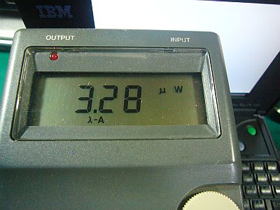
�d������300mA�i�}�Q[click]�j�ŁA�P�x�͂��悻����3μW�i�}�P�j�������B�iWVGA-TFT�̎Q�l�l�j
����d�͂́A�ő��1.5W�����A�ʏ�͂��̔������炢�ł������̂ł͂Ȃ����Ǝv���B
�������A�ʓrADJ�M����p�ӂ��Ȃ���Ȃ�Ȃ��̂ŁA���ꂪ�ʓ|���B�f�l�I�ɂ́AADJ=VCC(+3.3V)�����œ����������B
�i������ʂ����d�������炷���@�Ƃ��ẮADE�M����FET�ŎāAADJ�M������邱�Ƃ��A�\��������Ȃ��j
�|�|�|�|�|�|�|�|�|�|�|�|�|�|�|�|�|�|�|�|�|�|�|�|�|
![�}�R�F�uAT050TN23V.1�v���ʕی�̂��߃t�B������@�@[click]���}�S�F���p��Q�͏�����](fig/d5vgatfc.jpg)
�{�{�{�@�����@�{�{�{
���́uVGA-TFT���W���[���iAT050TN23 V.1�j�v�́A������H��ʏ��PCB��ɁA�L���ʐς��g���đg��ł���B
�������A�����ی삷��g���A���͑S�̂��͂��Ă��āA"���W���[�����̂̌���"�������Ă��܂��Ă���B
���ꂪ�A��X�́u���p��v���A���W���[���̗����ɒu���Ȃ��j�Q�v���ɂȂ��Ă���B
���́A���܂Ŏg���ė����uWVGA-TFT���W���[���v�́A��3cm����FPC��ɑg��ł����āA���ʂ̐�L�ʐς�����قǑ傫���͂Ȃ��B
������A�u���p��v��u�����Ƃ��o�����킯���B
������A���S�����͐�̉ۑ�Ƃ��Ēu���A���ʂ́A���ʂ̊W�͂����ɓ�����m�F���邾���ɂ������B
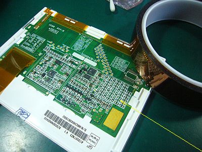
���̏ꏊ�ɁA�u���p��v2����u���ׂɁA�u�|���C�~�h�E�t�B�����v��B�i�}�R�j
2���́u���p��v�́A����"���\���"�̏�ɍڂ��ČŒ肷��B�i�}�S[click]�j
�X�ɁA���̊��ɂ́ALED�d���iDC-DC�R���o�[�^�j���u���悤�ɂ����B
���͑��u�R�l�N�^�v�ɂ́A����"�p�C���o�[�^"��������ė������̂��g���Ă���̂ŁA�{�̂̃o�b�N���C�g�p�d�����A���̂܂܍�����B
�i�d�����ɓ����Ă���"�Z���~�b�N�E�L���p�V�^"�͗L���Ȃ̂ŁA�c���Ă����Ηǂ������̂����A�p�[�c�ނ͑S���O���Ă��܂��Ă��āA�C���t���Ό�̍Ղ�j
�m��Z��Z�N������\�l���n
PC110�p 5�^VGA23-TFT�������A�]���@�@�@�@��English Note
![�}�T�FVGA-TFT�ŕ\���A�ꉞ�����@�@[click]���}�U�F��z���u���p��v�Ŏ��{](fig/d5vgatfe.jpg)
����́A�uPC110�v�{�̂Ɛڑ����āA�����ƕ\���o���邩�ǂ������������B
���̖{�̂́A���3��{���œZ�߂āA�i�K���Łj���������̂ŁA���́A����������"��"�E"�|"�E"�~"�Ɩ��t�����B
6���@�i"��"�F��ܐ�~-����i�j�A7���@�i"�|"�F��l��~-����i�E�s�����j�A8���@�i"�~"�F��O��~-�d���͓��邪�i�s�����j�ŁA�uPC110�v�{�̂Ƃ��āA7���@�i"�|"�j���g�����Ƃɂ����B
���A�g���C����5�^VGA-TFT�uAT050TN22 V.1�v���ɂ͋�J�͖����āA�u���p��v�𐳂����ڑ����āA�O����2��̓d����p�ӂ��쓮������A�i�����̓g���u�������A�₪�āj�܂Ƃ��ȕ\�����o���I�i�}�T�j
��z���Ȃ̂ŁA"WVGA-TFT���W���[��"�ł��o�Ă����W�b�^���t���b�J�Ȃǂ͂��邪�A����́u���p��v��PCB���ʼn��P�͏o���邾�낤�B�i�}�U[click]�j
�\����́A�e�ӂŖ�2�`3mm���A���g�ʼnB����邪�A���̂܂܂ł����Ƃ��g���Ȃ��͖����������B
�ނ��A�����ɒu�������݂́u���p��v�́A���W��߂�ɂ͕s�����^�s�\������A���̂܂܂ł͎��p���͖����B
���p����ڎw���ɂ́A�����Ɛi�������˂Ȃ�Ȃ��B
�����A�ʓr�傫�Ȗ�������݂��Ă����B
���̃��W���[���́A�]����DSTN-LCD�̋쓮�p�ɏo�͂���Ă���d��+3.3V (VCC�p�j�A+5V (VLED�p�j�̓d���e�ʂ�����d�͏���炵���B
������A�P���Ɂu���p��v��ʂ������̕����ł́A��肭�s���Ȃ��B�����d�����������Ă��܂��āA"�\��"���o�Ȃ��̂��B
�ނ��A���̃W�����N"7���@�F�|" ���A����ق���J�������Ă��Ȃ���A�uVCC�v�̕��̓d�͂͋����o�����̂��낤�Ǝv���B
�uVLED�v�ɑ��āA�u�C���o�[�^�p�d���v�i10.5V�A300mA�ȏォ�H�j���g���āA�����5V�ɕϊ����ċ�������A�]�T�͂��肻�����B
�������A�����A���́u7���@�v�́A�q���[�Y�����ł���炵���A�o�͂��o�Ă��Ȃ��B
���́uPC110�v�Q���A�u�C���o�[�^�d���v�������Ă�����̂͏��Ȃ���������Ȃ��B
������A����́A���̓d���͎g��Ȃ��B
����̌����́A�ʂ́u�������艻�d���v��p���čs�����B
�֑������A���́uAT050TN23 V.1�v�̕\�����A�����Əo�Ȃ����ɂ́A�i"�|"�������H�ƐS�z�ɂȂ��āj�uWVGA-TFT���W���[���v�Ɍq���ς��āA�i�{�̖̂������j�m�F���Ă����B
�|�|�|�|�|�|�|�|�|�|�|�|�|�|�|�|�|�|�|�|�|�|�|�|�|
![�}�V�F3.3V���o��͂��̒[�q�@�@[click]���}�W�F���ׂ��|������2.5V�H�I](fig/d5vgatfg.jpg)
�{�{�{�@�uPC110�v�̕\�����쓮�\�͂́H�@�{�{�{
����7���@�F"�|"�iPC110�j�ł́A�uVGA-TFT���W���[���v�́uVCC�v�ƁuADJ�v���uPC110�v��+3.3V�o�͒[�q�Ɍq���i�}�V�j�ƁA�d����+2.5V�߂��܂ʼn������Ă��܂��B�i�}�W[click]�j
�o�b�N���C�g�p�̓d���iVLED)���A�O�����狟�����Ă���ƁA�uADJ�v�����̓d���ł��A�o�b�N���C�g�͓_����������B
�������A�uVCC�v�̕���������߂��Ă���ׁA�����\���͏o�Ȃ��B
�uVCC�v�����p�Ƃ��āA����+3.3V�ȊO�ɁA+5V�o�͒[�q�ł������Ă݂����A��͂����d���������ׂ��A�d����2.5V�߂��܂Ńh���b�v���Ă��܂��B
![�}�X�F��֗p�O���d������A3.3V��5.0V�������@�@[click]���}�P�O�F�C���o�[�^�p�d���͗��p�\�I�H](fig/d5vgatfi.jpg)
�{�{�{�@�O���d���ʼn^�p�@�{�{�{
���̃}�V���́u�C���o�[�^�d���v�i�}�P�O[click]�j����o�͂����Ă��Ȃ����Ƃ����������̂ƁA+3.3V�d�����A+5V�d�����A���ׂ��|����Ɠd�����}�~�����邱�Ƃ����������B
����́A�W�����N�E�}�V��������~�ނȂ����낤�B
������܂��A�O���́u�������艻�d���v�ŋ쓮���邱�Ƃɂ����B�i�}�X�j
�u�������艻�d���v����uVCC�i3.3V�j�v�ƁuVLED�i5V�j�v���������Ă��鎞�ɁA������"�d��"�ׂ���A�ȉ��̂��Ƃ��������B
�@��VCC�i3.3V�j�F0.16A
�@�@VCC�i2.7V�j�F0.26A
�@��VLED�i5V�j �F0.27A
�@�@VLED�i4V�j �F0.33A
�@�@VLED (3.5V)�F0.04A
�uVCC�v�́A���X�ɖ�2.7V�ʂ܂łȂ牺����ꂻ�������A������E�������ƁA�\����������B
����́uVCC�v����꒼���ƁA��������B
�uVCC�v�����������"�R���g���X�g"�������Ȃ�A������Ǝキ�Ȃ�B
�܂��A"�W�b�^"�Ȃǂ��A����ɉ����āA�����Ȃ����菭�Ȃ��Ȃ����肷��B
�uVLED�v�̓d���́A���d�l���ł́Amin4.8V�ƂȂ��Ă��邪�A����7���@�F"�|"�ł́A�i�r���ŁA���ٓ_�����邪�jmin3.5V�܂ʼn�����ꂽ�B
���̎��̉�ʂ́A�N���ł͂��邪�A�Â��I
�܂�A���̕��@�ł��A�P�x�������o�������Ɏv����B
�������A�r���ɓ��ٓ_������̂ŁA���܂�ǂ�������@�ł͂Ȃ���������Ȃ��B
�i���x�ƒ��́j�u�C���o�[�^�d���v�����A�����A�V�����q���[�Y�ƌ����^�T�T����A�����邾�낤�Ǝv���B
���邢�́A���̏C���̎��ɁA�q���[�Y�̑���ɁA��20���i1�`1.5W�j���̃h���b�p��R������A�K�v��5V�͎��o���邾�낤���A�d���ی�p�ɂ��Ȃ�B
�������A����5V����A�X��3.3V�����o�����Ƃ���Ȃ�A��R�ł͐ق��B
��͂�A�C���̎��ɁA�����Ɂi2�`3W�ʂ́j�u5V���M�����[�^�v�������Ȃ����ǂ�����������̂��������낤�B
�i�����A�d�����ɂ܂ŁA�{�̂�����̂́A�C���i�܂Ȃ��Ȃ��j
![�}�P�P�Fct65535c�ł͉E�[�ŕ����������N���Ă���@�@[click]���}�P�Q�Fct65535v�ł͐���](fig/d5vgatfk.jpg)
�{�{�{�@VGA��ʂɂ��ĕ����������Ɓ@�{�{�{
���܂ŁAWVAG��ʂł́A������ƕ\������Ă����̂ŋC���t���Ȃ��������AVGA��ʂɂ���ƁA"ct65535c"�ł́A��ʂ̉E�[�������邱�Ƃ����������B�i�}�P�P�j
������AMoonlight���������A�f�[�^�Q�i�N���b�N���g�����_�E��������Ȃǂ̏��u���������Ă���j�Œu��������"ct65535v"�ŕ\�������Ă݂�ƁA�E�[�͌����邱�ƂȂ��A�����ƕ\�������B�i�}�P�Q[click]�j
�����A���̏��A���҂ɂ͂��ꂼ��̖��_�������āA"ct65535c"�ł��t���b�J���ڗ����A"ct65535v"�ł��W�b�^���ڗ����Ƃ��B
"�W�b�^"�̕��́A�u���p��v��PCB������A�قږ�������悤�Ȃ̂ŁA������Ɋ��҂������B
�X�ɁAMoonlight�����"VPATCH"����������A"ct65535c"�́A�����ꂨ�������ɂȂ�^�����B
�������A�����Ŗ��_���������Ă���A�������͍��邱�Ƃ��Ȃ�����A���������g�������悤�B
����́AXR���W�X�^�̂ǂꂩ������A�����邾�낤�Ǝv���̂ŁA���̓��A�C�����悤�B
![�}�P�R�F�㉺���t�l���I�@�@[click]���}�P�S�F39,40�͋��ɁAVCC���x��](fig/d5vgatfm.jpg)
�{�{�{�@�\�L�ԈႢ�H�@�{�{�{
���������Ȃ���A�mU to D�n��"GND"�A�mL to R�n��"VCC"�Ə����Ȃ���ڑ������̂����A�\�������Ă݂�ƁA�����t�l�I�H�i�}�P�R�j
���s���낵�Ȃ���A�q���ւ��Ă݂�ƁA�����Ƃ�"VCC"�������������B�i�}�P�S[click]�j
���̎����͎b�肾����������A�d�����Ȃ��̂��ȁH
�������A�d���l�ŁuTBD�v�������͍̂��������̂��B
�܂��ALED�̓d��-�P�x�����́A���i�����ŁA�܂�����͂��Ă��Ȃ��̂�������Ȃ����A���̃��W���[���́A�d�͏���ʂ��d������n���f�B�^�|�[�^�u���@�i�Ⴆ�A�i�r�@�j���[�J�ւ̔��荞�݂́A����̂ł͂Ȃ����ȁH�I
���ǁA�s��������́A�d�͏������ɂ��Ȃ�"�����u���^�@��"�����ɂȂ��Ă��܂��̂�������Ȃ��B
�m��Z��Z�N������\�����n
PC110�p 5�^VGA23-TFT�������A�Đi�@�@�@�@��English Note
![�}�P�T�F�f�������q���[�Y���p�i�Őڑ��@�@[click]���}�P�U�F���O�������ތQ](fig/d5vgatfo.jpg)
���́A����7���@�F"�|"��"VGA23-TFT��"�́A�d���s���̖���������āA��x�A�I�������߂��B
�����A�u�C���o�[�^�d���v���g����A�d�͕s���͉����o�����������A�����A���̃}�V���̓q���[�Y����Ă��āA���̓d�����g���Ȃ����炾�B
�����A�q���[�Y����u�C���o�[�^�d���v���r�I�e�ՂȎ菇�ŕ��������閭�Ă��v���t���āA����Ă݂����肭�s�����̂ŁA��R�A"VGA23-TFT��"��i�߂�ӗ~���A�N���ė����I
����̋L���́A���̎��|����̑O�i�K�܂ŁB
�u�C���o�[�^�d���v���q���[�Y��"��������C�i�����܂��͕t���j"����ɂ́A�uBeige-o-Vision�v����YouTube������q�����Ă�������悤�ɁA�w�����S�ɋ߂����܂ŕ������Ȃ���Ȃ�Ȃ��B
�������A����ȍ�Ƃ́A���ɂ͓�����A�����I���Ƃ��A�����Ɗy�ɏo���Ȃ����̂��H
�D�D�D��X�A8���@�F"�~"�́u�C���o�[�^�E�R�l�N�^�v���ォ��`����ʒu�ɂ������B
����ƁA�ʓr�A�u�d�����W���[���v�Ƃ��Ƃ炵���킵�Ă݂���A�i�Y�o���I�j�u�q���[�Y�v�̗��[�����������I
�Е��́A�R���f���T�̃v���X���ŁA����́A�ܘ_�A�R�l�N�^��No.1�s�����B
���̗������q���A�u�C���o�[�^�d���v�͕�����������I
�����ŁA����7���@�F"�|"����A�K�v�ŏ����̕��ށi���P�[�X�A�}�C�N�E�J�o�[�A�q���W�E�J�o�[�A�L�[�{�[�h�E�P�[�X�A�r�X�ށj�i�}�P�U[click]�j���O���A�u��C���i�v�c�t��������A�ēx�g�ݒ������B
�����Ɏ��t����u��C���i�v�Ƃ��āA���ꂱ��l�������A�ʏ�Ȃ�A���[�h���t���u�q���[�Y�v��������Ȃ��B
�����A����́A�i��X�A�W�����N���Ō��t��������R�j1.9����R�Őڑ������B�i�}�P�T�j
�����A���̓d����LED�d���i5V�A0.27A�j�Ɏg���ꍇ�A�d���~�����i10V-5V�j�^�K�v�d���i0.27A�j�̒�R�i��18���j�����Ă����A"�d���ی��"��"���M���U��"�ɂ��Ȃ�B
���邢�́A�o�͂Ƃ���+5V�����o���Ȃ�A500mA�`1A���x�́u3�[�q���M�����[�^�v��u�����Ƃ��K�v���B
������9mm�ȉ���"TO-126�^�p�b�P�[�W"�Ȃ�A���Ƃ��g�ݍ��߂邾�낤���A�����A300mA�̂��̂��������B
TO-220�^�Ȃ�A�d���e�ʂ͏\�������A�T�C�Y���傫�߂���B
�|�|�|�|�|�|�|�|�|�|�|�|�|�|�|�|�|�|�|�|�|�|��
![�}�P�V�F�d����̕��i�������@�@[click]���}�P�W�F�o�͓d���̊m�F](fig/d5vgatfq.jpg)
�{�{�{�@�[�q�̈ʒu�A�o�͂̊m�F�A�@�{�{�{
���c�t�����ׂ��[�q�̈ʒu�́A�i�}�P�T�́j"D30"�Ƃ����V���N����������钼���T���A�u�o�͕����R���f���T�i�ԐF�j�v�̃v���X10V�[�q���B�����āA���̒����ׂ��AGND�[�q�B�i�}�P�V�j
�{�̂̏ォ��A�e�X�^�_����������ŁA�e�[�q�𑪂�����A���ꂼ��̓d�����m�F�o����B
�q���[�Y��p�̒��R�Őڑ������o�͒[�q���A�[���̃R�l�N�^���ő�������A�ԈႢ�Ȃ�+10V���o�Ă����B�i�}�P�W[click]�j
�悵�I����Ȃ�A������A"TFT���W���[���p�d��"�Ƃ��Ďg���������I
�D�D�D���́A"VGA23-TFT"�����łȂ��A������A"6�^WVAG-TFT�p�d��"�Ƃ��ė��p�o���Ȃ������A�l�����B
�uPC110�v�ɂ���ẮA"�d�����̗͗ʕs��"�ŁA6�^WVAG-TFT���쓮�o���Ȃ����m�����邩�炾�B����ւ̑Ώ��Ɏg�������B
![�}�P�X�F�J�o�[��킹��ׂ́u���p��v�̔z�u�����@�@[click]���}�Q�O�F��z���p�̍ޗ��ƌ����\](fig/d5vgatfs.jpg)
�{�{�{�@�u���p��v������Ԃց@�{�{�{
"+10V�d��"���m�ۏo���邱�Ƃ����������̂ŁA�u���p��v�����W���[���̔w���ɎR�ς݂ɂ����A�����̋X�y�[�X�ɉ������ލH�v�����Ă݂��B
�����͋�������ǂ��A���Q��ςݏd�˂�����ɂ���A��z���Ȃ�A16�C17�{�ʂ̕t���͉\���낤�B�i�}�Q�O[click]�j
�u�R�l�N�^�t����v2��A2����؍�E���H���āA�uFFC�R�l�N�^�v�Ƃ̈ʒu���킹�����Ă݂��B�i�}�P�X�j
�E���̋�ԂɁA�s�̗̂����ȁuDC-DC�R���o�[�^�E���W���[���v��u�����Ƃ������A��10mm�Ȃ̂ŁA��1�A2mm���͂ݏo��B���̃^�C�v�́A�������ȁH
�����́A���������H�v��T�����K�v���ȁB
�m��Z��Z�N�����O�\���n
PC110�p 5�^VGA23-TFT�������A�d���@�@�@�@��English Note
![�}�Q�P�F ��z�����p���DC-DC�R���o�[�^��2���ځi5V, 3V�j�@�@[click]���}�Q�Q�F ���p��̕��ŁA�E�[����6�o������](fig/d5vgatfu.jpg)
�E���̋�ԂɁA�uDC-DC�R���o�[�^�v��2�u�����ƍl�������A��������Ȃ��̂ŁA��芸�����A���W���[���̔w���ɂ������Ƃɂ����B
����ƕ��s���āA�i�s�́E�����i�́j�u���p����v�������̋�Ԃɔ[�܂�悤�ɉ��H���āA��z���Ŏd�グ���B
�������āA�S�̂̓���m�F�����Ă������B
�uDC-DC�R���o�[�^�v�́A��ŏ����X�����Ȃ��̂��w�������̂ŁA����Ɠ���ւ�����A�����ƉE��ԂɎ��܂����B�i�}�Q�P�j�i2���V�Q�O�������݁j
����ɂ���āA�i���ڂ́j�uVGA-TFT���W���[���v�ŁA����Ɨ��J�o�[����邱�Ƃ��o�����B
���ʂ́A���������A�����̌����ݒʂ�A��ʂ̉E���� 6�o���A���g�ʼnB�����B�i�}�Q�Q[�N���b�N]�j
���́A�㉺��ʂ��A��3mm���B����Ă͂���̂����A�C�ɂ��Ȃ���A���̂܂܂ł��g�p�ɑς�����Ǝv���B
�Ƃ��낪�A���ꂪ���ڂɏo�āA�������̃V���[�g��U�����āA7���@�F"�|"�����S���Ă��܂����I
�|�|�|�|�|�|�|�|�|�|�|�|�|�|�|�|�|�|�|�|�|�|��
![�}�Q�R�F FFC�ƃR�l�N�^�̈ʒu���킹�@�@[click]���}�Q�S�F ��̉��H�Ǝ�z��](fig/d5vgatfw.jpg)
�{�{�{�@�u���p��v�̉��H�Ǝ�z���@�{�{�{
�i����܂ŁA��Ԃ̐��������ɍς�ł����j�����́u���p��v���A������ԂɎ��߂�ƂȂ�ƁA�؍���H���K�v�ɂȂ�B�i�}�Q�S[�N���b�N]�j
FFC�iFlexible Flat Cable�j�Ƃ̌�����Ԃ����āi�}�Q�R�j���Ȃ���A�ؒf���郉�C�������߂Đؒf���A�����̊�Ԃ��A��Ŕ��c�t�����āA�����z���������B
�������A�ǂ����Ă������ȏ��́A"FFC�̋Ȃ�"��"���W���[���ʒu"�̕ύX�ŁA�Ώ������B
���A�u30�s���A40�s���R�l�N�^�v�͗������A"�����s���^�h���g�p���Ă���B
�܂��A�z�������ԈႦ�Ȃ��悤�ɁA"�s���ԍ�"���ו����ň���������Ђ�t���Ă����āA���c�t���z���������B
�i���̂����ŁA�����1�{���z���ԈႢ�������ɍς�j
![�}�Q�T�F 5V�A3V��������@�@[click]���}�Q�U�F 5.0V��3.1V�ɐݒ�](fig/d5vgatfy.jpg)
�{�{�{�@2�d���̐ݒ�A�����Ď��S�@�{�{�{
�g�����uDC-DC�R���o�[�^�v�́A�����^��"�~���^�̃��W���[��"�ŁA�d���e�ʂ͕s�������A300mA���x�͎���Ǝv���B
�����́A���Œ�VR�Œ������\�Ȃ̂ŁA�i�Œ莮�ɂ����j�uADJ�v��I�������B
�i�uEN�v�[�q�́A���u�̂܂܂ŁA�ǂ��悤���j
���A3V�̕��́A�ʏ�Ȃ�+3.3V�ɐݒ肷��̂��퓹�����A���́uAT050TN23 V.1�v�ł́A���������������A�m�C�Y�^�W�b�^������悤�Ȃ̂ŁA���悻3.1V�ɐݒ肵���B�i�}�Q�T�j
����ŁA�\�����o��悤�ɂ��āA������"�G�[�W���O"�����Ă݂����A���Ɉُ�͌����Ȃ������B
���̌�ALCD�P�[�X�����āA����Ɗ����̎p���m�F�����B�i�}�Q�U[�N���b�N]�j
�D�D�D�Ƃ��낪�A���̍ہA�u���p��v�ƃ��W���[���̋������Ƃ̊ԂŁA���������V���[�g�����炵���A�₪�āA�\�����o�Ȃ��Ȃ�A�{�̂�����ɓ����Ȃ��Ȃ��Ă��܂����B
���Ƃ܂��A����7���@�F"�|"���A"�s���W�����N"�̒��Ԃɓ����Ă��܂����I�i�g�z�z�j
�m��Z��Z�N�㌎�O�\���n
PC110�p 5�^VGA23-TFT�������A�C���@�@�@�@��English Note
![�}�Q�V�F�C������AT050TN23V.1�̐ڑ����@[click]���}�Q�W�F�f���ӏ����A�X�ɔj�����C���s�\�ɂȂ��Ă���](fig/d5vgatz1.jpg)
���́A7���@�F"�|"�͎���ł͂��Ȃ������B�i���̌�F�������j
���݂��A���h���e�X�g�x���`�����ʂ����Ă���Ă���B
�Ƃ��낪�A����"�x���`"�Łuct65535d.exe�v���e�X�g���Ă��鎞�ɁA�uAT050TN23V.1�v����C����FPC�̒f�������A�Ăђf�����ďC���s�\�ɂȂ��Ă��܂����B�i�}�Q�W�m�N���b�N�n�j
����́A����"�f��FPC"�����āA��p�^�[���ɁA���ځu0.5mm�s�b�` ���s���^40�s���E�R�l�N�^�v�c�t������Ƃ������@�ŁA�C�����Ă݂��B�i�}�Q�V�j
���ʂ́A��肭�s�����悤�ŁA�C���E�ڑ��́A�����I�H
�u�R�l�N�^�v�́A����ɍׂ����ʃe�[�v��~���A���̏�ɒ���t����悤�ɁA�Œ肵���B
�i���̌�ŁA�s���Q�̔��c�t���������j
�܂��A�u�R�l�N�^�v�������A"�؍H�p�{���h"�ŗ��߁A�X�ɁA�u�|���C�~�h�E�e�[�v�v�ʼn�����悤�ɂ����B
�i�����A�ǂ̒��x�̌Œ苭�x�����邩�͕s�������j
�|�|�|�|�|�|�|�|�|�|�|�|�|�|�|�|�|�|�|�|�|�|��
![�}�Q�X�F���i�ʐ^��\������AT050TN23V.1�@�@[click]���}�R�O�F�R�l�N�^�̗����AFPC�����M���������ہA�t���ɉe�����o���͗l](fig/d5vgatz3.jpg)
�{�{�{�@�C���̌��Ɖe�@�{�{�{
7���@�F"�|"�ƌq���ŁA���̕\���������B
"ct65535d.exe"�̗nj��ʂ������āA������ʁA�摜��ʋ��ɁA�W�b�^���t���b�J�������A�N���ɕ\���o���Ă���B�i�}�Q�X�j
�������A�c�O�����A���x�R�l�N�^�̉��ӂ�ɁA�Â��e���o�Ă���B�i�}�R�O�m�N���b�N�n�j
����́A�ǂ����u�R�l�N�^�v��uFFC�v���e�[�v�ʼn����t���Ă���̂ŁA���̈��͂ʼnt���K���X���c��ł���ׂ炵���B
�������ɂ߂āA��������Ήe�͏����邾�낤���A�u�R�l�N�^�v�̌Œ�͂𗎂Ƃ��̂ŁA���̏��u�͕ۗ����Ă��������B
�܂��A�M�d�ȁuVGA23-TFT���W���[���v���A�����Ԃ��������ŁA�D���Ƃ��悤�I
�|���|���|���|���|���|���|���|���|���|���|���|���|���|���|���|���|���|���|���|���|���|
5-inch VGA23-TFT for PC110 Examination Start
Mr.Moonlight found out the (easier to use) 5-inch VGA-TFT module "AT050TN23V.1.
So I was ordering from a "Hong Kong store" (via "eBay") and it arrived in a few days. (\8,359 shipping and handling included. items: $40, shipping $35, etc.)
This module is different from "AT050TN22 V.1" in the previous section.
Only two power systems "VCC" and "VLED" are available, making it easy for us amateurs to use.
The number of pins on the "connector" is also grouped into 40 pins like "WVGA-TFT", but there is no "touch panel/digitizer".
Since the "GND line" is sandwiched between the color signal lines, the "relay board" for WVGA-TFT cannot be used as it is.
(Reference material by Mr.Moonlight)
Since we are not in the stage of making "PCB" yet, we plan to make "relay board" by hand wiring.
But before that, what to do with "backlight power supply" is a big issue.
This time, I briefly examined its characteristics.
The voltage is limited to +5V, and it seems that the brightness is changed by the duty ratio of the ADJ signal.
The current was about 300mA (Fig_2 : click) and the brightness was about average 3μW (Fig. 1). (WVGA-TFT reference value)
The maximum power consumption is about 1.5W, but I think that about half of this is usually enough.
However, it is troublesome because you have to prepare an ADJ signal separately. For amateurs, I want to work only with ADJ=VCC(+3.3V).
(As a way to reduce the current by a certain amount, it may be possible to receive the DE signal with a FET and create the ADJ signal)
�|�|�|�|�|�|�|�|�|�|�|�|�|�|�|�|�|�|�|�|�|�|��
+++ Preparation +++
This "VGA-TFT module (AT050TN23 V.1)" has a built-in internal circuit on a normal PCB with a large area.
Moreover, the frame that protects it surrounds the periphery, increasing the "thickness of the module".
This is an obstacle that prevents us from placing our "relay board" behind the module.
Actually, the "WVGA-TFT module" I have been using so far is built on an FPC with a width of about 3 cm, and the area occupied by the back side is not so large.
That's why I could put the "relay board".
Again, we will put complete encapsulation as a previous issue, and for the time being, we would like to check the operation without covering the back cover.
Put "polyimide film" to place two "relay boards" in this place. (Fig_3)
The two "relay boards" are placed and fixed on a thin "universal board". (Fig_4 [click])
Furthermore, the LED power supply (DC-DC converter) is also placed on the board.
Since the input "connector" is the one cut out from the original "waste inverter", the power supply for the backlight of the main unit can be directly connected.
(The "ceramic capacitor" that was in the power supply was effective, so I should have left it, but all the parts have been removed.)
[August 24th, 2020]
5-inch VGA23-TFT for PC110 Review, Evaluation
![Fig_5: Displayed on VGA-TFT, completed once [click]��Fig_6: hand wiring relay board](fig/d5vgatfe.jpg)
This time, I tried connecting with "PC110" main body to see if it can actually display on the VGA-TFT module.
This main unit bought at a reasonable price with other 2 units +�� the other day, and I tentatively named them �gPine�h, �gBamboo�h, and �gPlum�h.
Unit 6 ("Pine": about \5,000 - working), Unit 7 ("Bamboo": about \4,000 - working, but some defective), Unit 8 ("Plum": about \3,000 - power is turned on, but not work) , I decided to use Unit 7 ("Bamboo") as the main body of "PC110".
This was not so difficult as I tried the last time, 5-inch VGA-TFT "AT050TN22 V.1".
I connected "relay board" properly with my soldering, and driving with prepared outside two kinds of power supplies, (although it was a little troubled, but soon) I got a decent display ! (Fig_5)
Since it is manual wiring, there are jitter and flicker which were also shown in "WVGA-TFT module", but this is it will be possible to improve by using PCB as the "relay board". (Fig_6 [click])
The display area is hidden by the window frame by about 2 to 3 mm on each side, but it seems that it can be used even if it is left as it is.
However, the current "relay board" placed on the back side is unsuitable/impossible to close the back cover, so it is not practical as it is.
To be practical, I have to evolve more.
However, there was a separate big problem.
This VGA module seems to consume more power than the current capacity of the power supply +3.3V (for VCC) and +5V (for VLED) output for driving the original DSTN-LCD.
Therefore, the method of simply connecting the "relay board" does not work.
The "display" does not appear because the supply voltage has dropped.
However, if this "Bamboo" does not have so much fatigue, I think that the power of "VCC" had be supplied.
If I use "Inverter power supply" (10.5V, 300mA or more ?) for "VLED", it will be possible to convert it to 5V and supply it.
However, unfortunately, this "Bamboo" seems to have a blown fuse, and no output is.
In other "PC110"s, the "inverter power supply" may not be active.
So, I don't use this power supply.
This time, I used another "DC stabilized power supply".
When the display of "AT050TN23 V.1" does not appear properly, I'm worried that this "Bamboo" has been destroyed ?
So I changed it to "WVGA-TFT module" and confirmed (the safety of the main body).
�|�|�|�|�|�|�|�|�|�|�|�|�|�|�|�|�|�|�|�|�|�|��
![Fig_7 : The terminal that should output 3.3V [click]��Fig_8 : 2.5V when a load is applied?!](fig/d5vgatfg.jpg)
+++ What is the display drive capacity of the �gPC110�h? +++
In the Unit 7 : "Bamboo" (PC110), set "VCC" and "ADJ" of "VGA-TFT module" to "PC110". When connected to the +3.3V output terminal (Fig_7), the voltage drops to near +2.5V. (Fig_8 [click])
If the power supply (VLED) for the backlight is supplied from the outside, the backlight can be turned on even if "ADJ" is at such low voltage.
However, since "VCC" is too low, nothing is displayed.
In order to supply "VCC", I also tried using +5V output terminal other than +3.3V, but the voltage drops to around 2.5V, probably because of the large current consumption.
Is the supply capacity of "PC110" much small ? Or is the consumption of "AT050TN23 V.1" much large ?
![Fig_9 : 3.3V and 5.0V are supplied from an external power supply [click]��Fig_10 : For inverter Power supply can be used !?](fig/d5vgatfi.jpg)
+++ Operated by an external power source +++
It was found that no output was coming from the "inverter power supply" (Fig_10 [click]) of this "Bamboo", and that both +3.3V and +5V power supply drastically dropped when a load was applied.
It's a junk machine, so it's inevitable.
This time also, I decided to drive it with an external "DC stabilized power supply". (Fig_9)
When "VCC (3.3V)" and "VLED (5V)" are being supplied from the power supply, I checked their "current", and the results were as follows.
�@*VCC (3.3V): 0.16A
�@�@VCC (2.7V): 0.26A
�@*VLED (5V): 0.27A
�@�@VLED (4V): 0.33A
�@�@VLED (3.5V): 0.04A
VCC" can be gradually lowered to about 2.7V, but when it goes below a certain limit, the display disappears.
This will be revived by reentering "VCC".
The higher the "VCC", the stronger the "contrast", and the lower it becomes weaker.
Also, "jitter" etc. will increase or decrease accordingly.
The voltage of "VLED" is min4.8V in the provisional spec., but in the Unit 7: "Bamboo" it was lowered to min3.5V (there is some singular point in middle way).
The screen at that time is clear but dark !
In other words, it seems that the brightness can be adjusted by this method as well.
However, it may not be a good control method because there is a singular point in the middle.
(Currently closed) "Inverter power supply", but maybe I can fix it if I replace it with a new fuse.
Or, at the time of repair, if I insert a dropper resistor of about 20 �� (1.0W ~ 1.5 W) instead of a fuse, I'll be able to take out the necessary 5V, and it will also be for power supply protection.
However, when I try to extract 3.3V from this 5V, it is not good with resistors.
After all, it would be wise to consider whether I can put a "5V regulator" (around 2 to 3W) here when repairing.
(But I don't feel like disassembling the main body to the power supply.)
![Fig_11 : ct65535c has a missing character at the right end [click]��Fig_12 : ct65535v is normal](fig/d5vgatfk.jpg)
+++ What I found on the VGA screen +++
Up until now, I did not notice that it was displayed properly on the WVAG screen, but when I switched to the VGA screen, I found that "ct65535c" lacked the right edge of the screen. (Fig_11)
When I try to display it with "ct65535v" which replaced with a data set by Mr. Moonlight, the right edge is displayed properly without being cut off. (Fig_12 [click])
However, as of now, both have their own problems.
In "ct65535c", flicker stands out, and "ct65535v jitter is noticeable in ".
"Jitter" can be almost eliminated by converting the "relay board" to a PCB, so I would like to expect that.
Furthermore, when Mr.Moonlight's "VPATCH" is completed, "ct65535c" will eventually become a payment box. It is.
However, if I know the problem, I'll not have any problems during the experiment, so let's continue using it for a while.
I think that this can be fixed by adjusting any of the XR registers, so I will fix it.

+++ Wrong notation? +++
While looking at the materials, I connected while saying "U" to "D" as "GND" and "L to R" as "VCC".
But, the screen was different situation. (Fig_11)
After trial and error, I tried to reconnect and found that "VCC" was the correct answer for both. (Fig_12 [click])
Since this document seems to be tentative, is there no help for it ?
However, it is a problem that there are many "TBD" in the current value.
Well, the current-brightness characteristics of LEDs may be moving improve on day by day and may not be stable yet.
However, does this module not difficult to attack the market of handy/portable device (eg, navigation device) manufacturers who place importance on power consumption ?
After all, the destination may be for "stationary equipment" where power consumption is not a problem.
[August 28, 2020]
5-inch VGA23-TFT for PC110 Study and Resume
![Fig_15 : Connect a blown fuse with a substitute [click]��Fig_16 : Removed parts group](fig/d5vgatfo.jpg)
Actually, this No.7:"Take / Bamboo"'s "VGA23-TFT" has a power shortage problem, so I decided to end it.
If the "inverter power supply" can be used, it seems that the power shortage can be resolved, but unfortunately, this No.has a blown fuse and its power supply cannot be used.
However, I came up with a good idea to restore (a fuse blowed)"Inverter power supply" with a relatively easy procedure, and when I tried it, it went well, so suddenly "VGA23-TFTized motivation to proceed"" came up !
This article is up to the stage before the work.
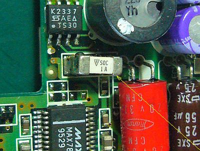
To correctly repair (replace or add) the fuse of the "inverter power supply", As we can see on the YouTube video of "Beige-o-Vision, assemble might be almost completely decomposed.
However, this kind of work is difficult for me ! Is there something I can do more comfortably ?
... Coincidentally, No.8:"Ume / Plum"'s "inverter connector" was in a position that could be seen from above.
Also, when I compare it with power module, it was (severely !) both ends of the fuse. I found !
One is the positive side of the capacitor, and the other is, of course, the connector No.1 pin.
"Inverter power supply" can be restored by connecting both point !
So, from this No.7: "Take / Bamboo", remove the minimum necessary components (Bottom case, Microphone cover, Hinge cover, Keyboard case, screws) (Fig_16 [click]), and perform "Repair". After re-assembling the parts, they were reassembled.
I thought about this as a "repair part" to be attached here, but in the normal case, it may be a "fuse" with a lead wire.
But this time, I connected it with a 1.9�� resistor (a small resistor I found in a junk box by chance). (Fig_15)
If this power supply is used for LED power supply (5V, 0.27A), insert a voltage drop (10V-5V)/required current (0.27A) resistance (about 18��) If you do so, it will also be a "power protection measure" and a "heat dissipation dispersion measure".
Or, if you want to take out +5V as an output, you need to put a "3 terminal regulator" of about 500mA to 1A.
The "TO-126 type package" with a width of 9mm or less could be incorporated, but it's not over 300mA when I add the +3.3V supply.
The "TO-220 type" has sufficient current capacity, but its size is too large.
�|�|�|�|�|�|�|�|�|�|�|�|�|�|�|�|�|�|�|�|�|�|��
+++ Terminal position, output confirmation +++
The position of the terminal to be soldered is (of Fig_15) "D30", right next to the silk-printed area, the plus 10V terminal of the "output smoothing capacitor (red)". And right next to it is the GND terminal. (Fig_17)
From the top of the main unit, insert the tester bar and measure each terminal, then I could check each voltage.
When I measured the output terminal connected with a low resistance as a substitute for the fuse at the connector side at the end, it was definitely +10V. (Fig_18 [click])
Alright! If this is the case, you can use this as a "power supply for the TFT module"!
�D �D �D Actually, we are considering not only "VGA23-TFT" but also this "6-inch WVAG-TFT power supply".
This is because, depending on "PC110", the 6-inch WVAG-TFT cannot be driven due to "insufficient power supply". It can be used to deal with it.
![Fig_19 : rearrangement of relay board [click]��Fig_20 : parts of hand wiring and the diagram](fig/d5vgatfs.jpg)
+++ "Relay board" to the left space ++
I found that "+10V power" could be secured, so I tried to push the "relay board" into the empty space on the left side instead of stacking it on the back of the module.
Although the width is narrow, if you use a method of stacking wire groups, you can connect about 16 or 17 wires if you use manual wiring. (Fig_20 [click])
I tried cutting and processing 2 types of "PCB with connector" and aligning with "FFC connector". (Fig_19)
I tried to put a commercially available low-priced "DC-DC converter module" in the space on the right side, but since it is 10 mm wide, it protrudes about 1 or 2 mm. Is this type impossible ?
I need a little more ingenuity and exploration here.
[August 30th, 2020]
5-inch VGA23-TFT conversion for PC110 Consideration, power supply
![Fig_21 : Hand wiring relay board and two DC-DC converters installed (5V, 3V) [click]��Fig_22 : The width of the relay board is about 6mm at the right end](fig/d5vgatfu.jpg)
I thought of putting two "DC-DC converters" in the empty space on the right side, but I decided to put them on the back of the module because the width was not enough.
At the same time, the "relay board" (commercially available/off-the-shelf) was processed so as to fit in the space on the left side, and finished by hand wiring.
The operation of the whole was confirmed by combining them.
I bought a little slimmer DC-DC converters later, so I replaced it and it fits in the right space. (Fig_21) (2 pieces \720 including shipping)
As a result, I was able to finally close the back cover with the (thick) "VGA-TFT module".
The result is Success, but as expected, the right side of the screen is hidden by a window frame by about 6 mm. (Fig_22 [click])
Actually, the upper and lower screens are hidden by about 3mm each, but if I don't mind, I can still use them as they are.
However, it backfired and triggered a short circuit somewhere, and No.7:"Bamboo" died. !!
�|�|�|�|�|�|�|�|�|�|�|�|�|�|�|�|�|�|�|����
![Fig_23 : FFC and connector alignment [click]��Fig_24 : PCB processing and manual wiring](fig/d5vgatfw.jpg)
+++ Processing of "relay board" and manual wiring +++
Even a ready-made "relay board" (which used to be free of space restrictions) needs to be cut when it is placed in a narrow space. (Fig_24 [click])
Taking into consideration the state of connection with an FFC (Flexible Flat Cable) (Fig_23), the line to be cut was determined and cut, and both boards were soldered by hand to form a connection wiring.
However, if it was impossible, I dealt with it by changing "FFC bending" and "module position".
Both "30-pin and 40-pin connectors" use the "lower pin type".
Also, in order not to make a mistake in the wiring location, a piece of paper with the "pin number" printed in fine letters was attached, and the wiring was done by soldering.
(Thanks to that, I did not make any wiring mistake this time��)
![Fig_25 : 5V �� 3V series method (using MP1584EN) [click] �� Fig_26 : 5.0 Set to V and 3.1V](fig/d5vgatfy.jpg)
+++ 2 power supply settings, and death +++
The "DC-DC converters" I used is an ultra-compact "buck-down module" whose current capacity is unknown, but I think it can get about 300mA.
These are adjustable with semi-fixed VR, so I chose "ADJ" (not fixed).
(The "EN" terminal seems to be good as it is.)
For 3V, it is normal to set it to +3.3V, but in my "AT050TN23 V.1", lowering it will reduce noise/jitter, it set to about 3.1V. (Fig_25)
With this, I tried to "aging" for several hours with the message displayed, but nothing unusual was seen.
After this, I set the LCD case and finally confirmed the appearance. (Fig_26 [click])
... However, at that time, it seemed that there was a short circuit somewhere between the "relay board" and the metal part of "the module", and eventually the display disappeared and the main body also stopped working properly.
Oh my god (Tohoho!), this No.7:"Bamboo" has also joined the immovable junk !
[2020/09/30]
5-inch VGA23-TFT for PC110 Examination and repair
![Fig_27 : Repaired AT050TN23V.1 connection part [click]��Fig_28 : The disconnection point, Further damaged and unrepairable](fig/d5vgatz1.jpg)
In fact, No.7: "Bamboo" wasn't dead. (It was my misunderstanding)
Even now, it plays a good test bench .
However, when testing " ct65535d.exe " on that "bench", " AT050TN23V.1 The repaired FPC disconnection part of was disconnected again and became irreparable. (Fig_28�mclick�n)
This time, I tried to repair it by peeling off the "disconnected FPC" and soldering the "0.5mm pitch lower pin type 40pins connector" directly to the board pattern. (Fig_27)
The result seems to have worked, repair and connection is perfect !?
The "connector" was fixed by laying a thin double-sided tape on the substrate side and sticking it on it. (After that, the pins were soldered)
In addition, both sides of the "connector" were fastened with "wood glue" and further covered with "polyimide tape".
(However, it is unknown how much fixing strength it has)
�|�|�|�|�|�|�|�|�|�|�|�|�|�|�|�|�|�|�|�|�|�|
![Fig_29 : AT050TN23V.1 for displaying landscape photos [click]��Fig_30 : Back side of connector, It seems that the liquid crystal was affected when the FPC was heat-peeled.](fig/d5vgatz3.jpg)
+++ light and shadow after repair +++
I connected it to No.7:"Bamboo" and saw the display.
Due to the good effect of " ct65535d.exe ", both on the character and the image screen, there was no flicker and jitter , so it could be displayed clearly. (Fig_29)
However, unfortunately, a dark shadow appeared just behind of the connector. (Fig_30 [click])
It seems that this is because the "connector" and "FFC" are pressed with "polyimide tape", and the liquid crystal glass is distorted by the pressure.
If I loosen them and float them, the shadows will disappear, but it will reduce the fixing force of the "connector", so I would like to suspend the treatment.
Well, the precious " VGA23-TFT module " has just come back to life, so let's like it!
![�}�P�F�P�x�͕���3μW�@�@[click]���}�Q�F�d���͖�300mA](fig/d5vgatfa.jpg)
![�}�R�F�uAT050TN23V.1�v���ʕی�̂��߃t�B������@�@[click]���}�S�F���p��Q�͏�����](fig/d5vgatfc.jpg)
![�}�T�FVGA-TFT�ŕ\���A�ꉞ�����@�@[click]���}�U�F��z���u���p��v�Ŏ��{](fig/d5vgatfe.jpg)
![�}�V�F3.3V���o��͂��̒[�q�@�@[click]���}�W�F���ׂ��|������2.5V�H�I](fig/d5vgatfg.jpg)
![�}�X�F��֗p�O���d������A3.3V��5.0V�������@�@[click]���}�P�O�F�C���o�[�^�p�d���͗��p�\�I�H](fig/d5vgatfi.jpg)
![�}�P�P�Fct65535c�ł͉E�[�ŕ����������N���Ă���@�@[click]���}�P�Q�Fct65535v�ł͐���](fig/d5vgatfk.jpg)
![�}�P�R�F�㉺���t�l���I�@�@[click]���}�P�S�F39,40�͋��ɁAVCC���x��](fig/d5vgatfm.jpg)
![�}�P�T�F�f�������q���[�Y���p�i�Őڑ��@�@[click]���}�P�U�F���O�������ތQ](fig/d5vgatfo.jpg)
![�}�P�V�F�d����̕��i�������@�@[click]���}�P�W�F�o�͓d���̊m�F](fig/d5vgatfq.jpg)
![�}�P�X�F�J�o�[��킹��ׂ́u���p��v�̔z�u�����@�@[click]���}�Q�O�F��z���p�̍ޗ��ƌ����\](fig/d5vgatfs.jpg)
![�}�Q�P�F ��z�����p���DC-DC�R���o�[�^��2���ځi5V, 3V�j�@�@[click]���}�Q�Q�F ���p��̕��ŁA�E�[����6�o������](fig/d5vgatfu.jpg)
![�}�Q�R�F FFC�ƃR�l�N�^�̈ʒu���킹�@�@[click]���}�Q�S�F ��̉��H�Ǝ�z��](fig/d5vgatfw.jpg)
![�}�Q�T�F 5V�A3V��������@�@[click]���}�Q�U�F 5.0V��3.1V�ɐݒ�](fig/d5vgatfy.jpg)
![�}�Q�V�F�C������AT050TN23V.1�̐ڑ����@[click]���}�Q�W�F�f���ӏ����A�X�ɔj�����C���s�\�ɂȂ��Ă���](fig/d5vgatz1.jpg)
![�}�Q�X�F���i�ʐ^��\������AT050TN23V.1�@�@[click]���}�R�O�F�R�l�N�^�̗����AFPC�����M���������ہA�t���ɉe�����o���͗l](fig/d5vgatz3.jpg)


![Fig_5: Displayed on VGA-TFT, completed once [click]��Fig_6: hand wiring relay board](fig/d5vgatfe.jpg)
![Fig_7 : The terminal that should output 3.3V [click]��Fig_8 : 2.5V when a load is applied?!](fig/d5vgatfg.jpg)
![Fig_9 : 3.3V and 5.0V are supplied from an external power supply [click]��Fig_10 : For inverter Power supply can be used !?](fig/d5vgatfi.jpg)
![Fig_11 : ct65535c has a missing character at the right end [click]��Fig_12 : ct65535v is normal](fig/d5vgatfk.jpg)

![Fig_15 : Connect a blown fuse with a substitute [click]��Fig_16 : Removed parts group](fig/d5vgatfo.jpg)

![Fig_19 : rearrangement of relay board [click]��Fig_20 : parts of hand wiring and the diagram](fig/d5vgatfs.jpg)
![Fig_21 : Hand wiring relay board and two DC-DC converters installed (5V, 3V) [click]��Fig_22 : The width of the relay board is about 6mm at the right end](fig/d5vgatfu.jpg)
![Fig_23 : FFC and connector alignment [click]��Fig_24 : PCB processing and manual wiring](fig/d5vgatfw.jpg)
![Fig_25 : 5V �� 3V series method (using MP1584EN) [click] �� Fig_26 : 5.0 Set to V and 3.1V](fig/d5vgatfy.jpg)
![Fig_27 : Repaired AT050TN23V.1 connection part [click]��Fig_28 : The disconnection point, Further damaged and unrepairable](fig/d5vgatz1.jpg)
![Fig_29 : AT050TN23V.1 for displaying landscape photos [click]��Fig_30 : Back side of connector, It seems that the liquid crystal was affected when the FPC was heat-peeled.](fig/d5vgatz3.jpg)